Frequency Synthesizer Circuit Diagram A frequency synthesizer uses phase-locked loop (PLL) to generate output frequencies over a wide range. The typical range is from 1 MHz to 160 MHz. Fig: Block diagram of a frequency synthesizer. As illustrated in the block diagram above, the key components of the frequency synthesizer are: Crystal oscillator; Phase detector; Low-pass filter The Fig. 2.130 shows the Frequency Synthesizer Block Diagram. It is similar to frequency multiplier circuit except that divided by M network is added at the input of phase lock loop . The frequency of the crystal-controlled oscillator is divided by an integer factor M by divider network to produce a frequency f osc /M, where f osc is the

High Speed Communication Circuits and Systems Lecture 18 Design and Simulation of Frequency Synthesizers Michael H. Perrott April 9, 2004 M.H. Perrott Outline Closed-Loop Design of Frequency Synthesizers-Introduction-Background on Classical Open Loop Design Approach-Closed Loop Design Approach-Example and Verification-Conclusion
Arduino Frequency Synthesiser Using 160MHz Si5351 Circuit Diagram
2:00 - 3:30 RF front-end design - LNA, mixer 4:00 - 5:30 Frequency synthesizer design I (PLL) T d J l 22 2008Tuesday, July 22, 2008 9:00 - 10:30 Frequency synthesizer design II (VCO) 11:00 - 12:30 RFIC design for wireless communications 2:00 - 3:30 Analog and mixed signal testing Frequency synthesizer design I (PLL), FDAI, 2008 2
The actual design is best done with the computer program. A more complex filter as an application is shown in Figure 4. Fig. 4 — Phase/frequency comparator and loop for the 72 to 92 MHz frequency synthesizer. A detailed overview on how to design a synthesizer is found in the book, Microwave and Wireless Synthesizers: Theory and Design, the design of a frequency synthesizer in a transceiver environment, from the mapping of standard-specifications to its integrated circuit implementation in a CMOS technology. The results show that careful system level planning leads to high-performance realizations of the synthesizer. A strategy of using different supply voltages to enhance The RF frequency synthesizer design involves the integration of a Phase-Locked Loop (PLL) and a Voltage-Controlled Oscillator (VCO) to generate stable and tunable radio frequency signals. The synthesizer includes a control interface for user adjustments. RF frequency synthesizers are the cornerstone of modern communication systems, ensuring
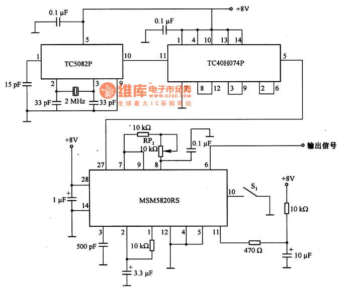
PDF Lecture 8 Frequency Synthesizer PLL Circuit Diagram
a reference frequency fref, the division ratios of N and R, and the frequency fmix, applied to the mixer to down-convert the signal; the resulting output frequency, f out, will be out fref fmix R N f + = ⋅ Equ. 4 The main benefit of this method is the improved noise performance due to the reduced division in the loop. Loop Filter Design
